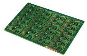
Multi-layer Benefits
From a technical point of view, multi-layer PCBs present several advantages in design. These benefits multi-layer PCBs present include:
• Small Size: One of the most prominent and lauded benefits of using multi-layer PCBs lies in their size. Because of their layered design, multi-layer PCBs are inherently smaller than other PCBs with similar functionality. This presents a major benefit to modern electronics, as the current trend is working toward smaller, more compact yet more powerful gadgets like smartphones, laptops, tablets and wearables.
• Lightweight Construction: With smaller PCBs comes less weight, especially as the multiple connectors required to interlink separate single and double-layered PCBs are eliminated in favor of a multilayered design. This, again, is beneficial for modern electronics, which are geared more toward mobility.
• High-Quality: Due to the amount of work and planning that must go into the creation of multilayer PCBs, these types of PCBs tend to be better in quality than single and double-layer PCBs. They also tend to be more reliable as a result.
• Increased Durability: Multilayer PCBs tend to be durable by their nature. Not only do these multilayer PCBs have to withstand their own weight, but they must also be able to handle the heat and pressure used to bind them together. On top of these factors, multilayer PCBs use multiple layers of insulation between circuit layers, binding it all together with prepreg bonding agent and protective materials.
• Enhanced Flexibility: Though this does not apply to all multilayer PCB assemblies, some do use flexible construction techniques, resulting in a flexible multilayer PCB. This can be a highly desirable trait for applications where mild bending and flexing may occur on a semi-regular basis. Again, this does not apply to all multilayer PCBs, and the more layers incorporated into a flexible PCB, the less flexible the PCB becomes.
• More Powerful: Multilayer PCBs are extremely high-density assemblies, incorporating multiple layers into a single PCB. These close-quarters enable boards to be more connective, and their innate electrical properties allow them to achieve greater capacity and speed despite their smaller size.
• Single Connection Point: Multilayer PCBs are designed to work as a singular unit, rather than in tandem with other PCB components. As a result, they have a single connection point, rather than the multiple connection points required to use multiple single layer PCBs. This proves to be a benefit in electronic product design as well since they only need to include a single connection point in the final product. This is particularly beneficial for small electronics and gadgets designed to minimize size and weight.
These benefits make multilayer PCBs highly useful in a variety of applications, particularly mobile devices and high-functioning electronics. In turn, with so many industries turning to mobile solutions, multilayer PCBs are finding a place in an increasing number of industry-specific applications.
Other news about S&L
- Celebrating the Establishment of SUNLYNN CIRCUITS(THAILAND)
- Good News! Sun&Lynn Circuits Co.,Ltd. is honored as one of the Top 100 Innovative Enterprises in Bao
- What Should You Know about Metal Core PCB
- FPC supplier : the types of Flexible PCB
- PCB manufacturer China:Why PCB board snake line, what is it used for?
- What is Metal Core PCB and types of Metal Core PCB?
- Why are High frequency PCBs much more expensive than normal PCBs?
- Flexible PCB supplier China :When to use flexible PCB?
- Flexible PCB manufacturer:What Is Flex Soldering?
- What Is Automotive PCB? Why we use automotive PCB?
Your browsing history
- Beijing's optoelectronic co., LTD
- What is the differnece between the Rigid Flex PCB and A Flexible Circuit
- SUCCESS
- Hikvision awarded S&L for the best PCB quality performance
- PCB factory china tells you the meaning of Tricolor column in front of barbershop?
- Rigid Flex PCB Supplier - What Is the Future of Advanced Electronic Manufacturing?
- See us at IPC APEX 2017
- Circuit board plant expansion in inland rushed upstream CCL factory halt the troops and wait
- PCB manufacturer China:Material Used in SMT Assembly
- PCBfactorychina:Huawei is to roll out 5.5G equipment!


A total of -comments【I want to comment】