PCB supplier china:What is PCB?
PCB supplier china:What is PCB?
Request PCB Manufacturing & Assembly Quote Now
Before we get to the most significant item in current times, we must look at the definition of making Circuit Boards that help us work with more enthusiasm;
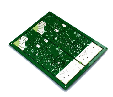
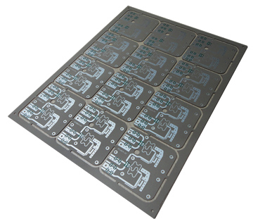
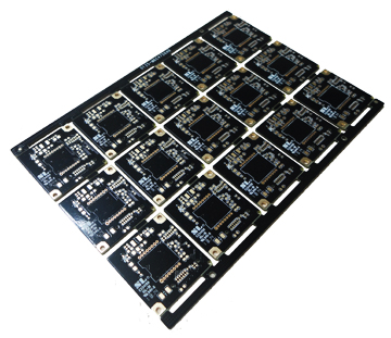
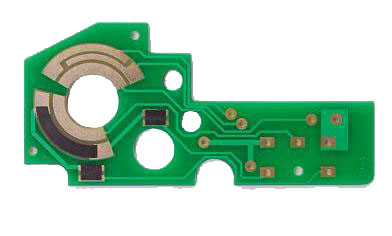
PCB supplier china:A printed circuit board(PCB) physically supports and links electrical parts electrically through conductive tracks, padding systems, and other components printed on a non-conductive substrate from copper sheets. A printed circuit board features copper traces pre-designed on a circuit.
PCB supplier china:You will learn how to make PCB at home. This will save you a lot of time from troubleshooting and double verifying the breadboard connections. After this session, you can even make your PCB. Just sit back and watch how!
1. Different Ideas to Make Own PCB at Home:
All three fundamental PCB techniques are available
- Method of Iron on Glossy paper
- The circuit on PCB by hand
- Machining laser edge etching.
Since the laser boards are a commercial DIY PCB approach, we shall examine the first two techniques for making PCBs at home in-depth.
2. List of Materials:
- Magazines or publicity pamphlets
- Laser Printer
- Household clothes Iron
- Copper laminate clad
- Solution Etching
- Kitchen scrubs
- Thinner, for example, acetone
- Coated plastic wire
3. Creating Layout for PCB:
This is usually done by turning the schematic chart of your circuit into your PCB layout utilizing software for the Pcb CIRUIT board. There are several open-source PCB layout and design software tools.
Some of them are mentioned here to start:
- Eagle Cadsoft
- PCBWizard
In Cadsoft Eagle, you may create your schematic circuit.
Request PCB Manufacturing & Assembly Quote Now
4. Get a Printout for PCB Layout:
Use the laser printer and the A4 photographic paper/glossy paper to print out your PCB layout. Keep the following considerations in mind:
- It would help if you held the reflection printout
- Select both the PCB software applications and the printer driver settings for the output in black
- Ensure the paper is printed on the magnificent side of the paper
5. Copper Plate Cutting:
Cut the copper board to the plan size. You have to pay good attention to the printing layout when you cut the copper plate as needed.
6. Use the Smoothing Scrub:
When you cut copper in the desired size, the edges are ruff; you may use a kitchen harsh sponge scrub to clean the copper side of the PCB by using stainless steel brush; this eliminates both the top oxide copper layer and the picture coating. A sanded layer makes the picture cling more effectively.
7. Print a Layout Design on Copper Plate:
Drawing a design on a copper plate is not a straightforward task since you can construct your DIY PCB flawlessly if you cannot create a design on the plate. You may use two strategies to tackle the challenge for this difficulty;
8. Circuit by using Permanent Marker:
Using the diagram picture references printed on glossy paper, construct a first basic drawing using a pencil and a black marker on a copper plate.
9. Iron on Glossy Paper:
Move from photo paper to the board the printed picture. Ensure the upper surface is flipped horizontally. Place the board’s copper surface on the printed pattern. Make sure the panel is correctly positioned along the edges of the printed pattern. Put a sheet on the two sides of the non-copper side of the board. This helps to keep the surface and the printed design in place.
10. How to use Iron:
We iron it on the copper side after printing on glossy paper. Heat the iron to the highest degree.
On either a clean wooden table and clothing, place the photopapers layout with the back of the photo paper towards you.
Grab one end of it by the napkin and place the hot iron for 10 – 20 seconds at the other end. Now iron the picture paper with the tip and use low pressure for around 5-15 minutes.
Be careful with the corners of the board – you have to push, iron it carefully.
The firm press for a long time appears to work more than Iron.
Iron temperature melts the glossy paper printed ink here and has been transferred to the copper plate.
Request PCB Manufacturing & Assembly Quote Now
11. Peeling off:
After ironing, pour warm water on the printed plate for about 10 minutes. Paper is softly dissolved and removed. With low angles & traces, remove the foil.
Sometimes, when the paper is removed, parts of the pattern becomes dim.
See, the figure in the check black line track is colored with light; hence the black marker is used for the dark track, as seen in the picture.
12. Etching the Chip:
Make pcb at home
- You must be attentive and cautious in this stage
- Put rubber or latex gloves initially.
- Place a newspaper to prevent the etching solution from spoiling the floor.
- Take a plastic container and add some water to it.
- Dissolve 2-3 tea cubes in the water with hydrochloric acid power.
- Soak the PCB for around 30 minutes to the Etching process (Ferric Chloride, Fecl3).
- Fecl3 interacts with copper unmasked and eliminates the undesirable copper from PCB.
- This is known as Etching. Use pins to remove the PCB and verify whether or not the entire exposed region has been grafted. If it is not etched, keep it in the liquid for some additional time.
- Rotate the plastic box carefully so that the solution of etching with visible copper and create iron and copper chloride interacts.
Check if all copper is etched after 2-3 minutes.
Now is the time to design some connections; in particular, we would like to link our LEDs and wire them in specific pins on the sockets to the capacitors. By choosing the Wire button, we accomplish this.
To create a wire, you click the starting point. Suppose you want to construct joints in the cable; you have to click and alter the direction. When you join your planned sections, use ESC to cancel and join more wires from the starting position.
13. Caution:
Do not contact the grafting data directly; always wear gloves before contacting the fluid.
When you notice copper gradually and then perfume following step.
14. Disposition:
The solution of Etching is hazardous to fish as well as other aquatic bodies.
Once you are done, don’t dump it down the sink. It is unlawful and might destroy your pipes.
Titrate of Etching and then remove the solution.
15. Link parts:
Now is the time to design some connections; in particular, we would like to link our LEDs and wire them in specific pins on the sockets to the capacitors. By choosing the Wire button, we accomplish this.
To create a wire, you click the starting point. Suppose you want to construct joints in the cable; you have to click and alter the direction. When you join your planned sections, use ESC to cancel and join more wires from the starting position.
16. Completion of connections:
Now that all our LEDs are ready for use, we can next concentrate on the buttons. We have to install more connections and resistors so that we can do anything. Just use the Insert tool to deliver1>GND to your base and the RE U>RE U 0207/10 to your capacitors. You may put them beneath the controls, as what is illustrated, to the schematic. Don’t forget to supply a 330-ohm value to each resistor.
Then the wire tool connects the base and the filters to leg three on each of the levers.
17. Adding Power to Schematic:
After that we have grounded our switches, we need some electricity. We go to source1 > +5V to click on our ADD button.
Then we put a source across each switch’s pin 1.
Now we can also use A2 to add a source and attach it to the A2-3 pin. Before inserting, you may rotate the component placement using a right-click before installation.
Request PCB Manufacturing & Assembly Quote Now
18. Error Checking:
Now that our design has been done, we will examine our mistakes on tools>ERC.
You will notice several mistakes, even though we did everything perfectly.
All these errors may be ignored since not all wires need to be attached, as previously stated. As an additional point, you don’t require LEDand Switch settings. Click on each “error” and hit each of the Approve buttons. Rerun the mistake repair to ensure that nothing else is incorrect. Watch for “matching wires” and other mistakes. The only ones we accept in the photo below.
Diy circuit board
19. Installation of the circuit:
Observe how we have our pieces right beside a box on a screen in a confusing mess. The container is where our circuit is going. For our Machine tool, we have to position these pieces in a logical design to grind it and install the circuit board on a Microcontroller and get it working correctly. This is primarily an afterthought for everything else, but the port orientation is essential to our connections. We require a certain distance between them and have connections A1 and A2 parallel to D1 and D2 c. The remainder of the components run between the two connection rows.
20. Final Touch:
Just several drops of thinner (nail polish solution works well) can altogether remove the toner on a scoop of cotton wool and return the copper area to it. Rinse well and wash with a clean towel or paper in the kitchen. Cut into final size and sand to polish edges. Solvent helps to attach glossy paper to stiff paper.
Finding:
The iron Glossy paper technique is an effective way of building a PCB at home. Each track may be reproduced flawlessly if done correctly.
Circuit by hand on PCB is restricted to our aesthetic abilities. This approach may easily be used for a small circuit; however, Iron-on Glossy Paper is preferable for complicated PCBs.
Other news about S&L
- Celebrating the Establishment of SUNLYNN CIRCUITS(THAILAND)
- Good News! Sun&Lynn Circuits Co.,Ltd. is honored as one of the Top 100 Innovative Enterprises in Bao
- What Should You Know about Metal Core PCB
- FPC supplier : the types of Flexible PCB
- PCB manufacturer China:Why PCB board snake line, what is it used for?
- What is Metal Core PCB and types of Metal Core PCB?
- Why are High frequency PCBs much more expensive than normal PCBs?
- Flexible PCB supplier China :When to use flexible PCB?
- Flexible PCB manufacturer:What Is Flex Soldering?
- What Is Automotive PCB? Why we use automotive PCB?
Your browsing history
- What are the options for metal core PCBs
- What is Health care PCB routing?
- Flexible PCB supplier China :How to Judge Whether The FPC is Good or Bad?
- Flexible PCB manufacturer:What is Flexible PCB?
- How to corerct solder balls before occurrence for Health care PCB
- Flexible PCB manufacturer tells you How to Solder Flex Circuit Boards by Hand (DIY)?
- PCB supplier China:Understand the past and present lives of PCB circuit boards
- POWERONE
- Flex rigid PCB manufacturer talk Rigid PCB Vs Flex PCB: What Is The Difference?
- What Should You Know about Metal Core PCB


A total of -comments【I want to comment】